Charge trap technology advantages for 3D NAND flash drives
Flash drive cells based on charge trap technology have several advantages over older floating gate cells. However, take note of potential reliability issues.
Over the past 10 years the storage industry has undergone a quiet transformation, fueled in large part by the proliferation of 3D flash. Prior to 3D, most flash SSDs used floating gate cells to store data, but now most of them are built on a 3D architecture that incorporates charge trap cells.
Charge trap flash offers better endurance and scalability and is less susceptible to damage and leakage. Charge trap cells also consume less energy and are faster to program.
Despite their benefits, the switch to charge trap cells has come with little fanfare, perhaps in part because they also bring challenges, particularly with reliability. For this reason, some manufacturers have stuck with floating gate cells and use them mostly for planar NAND, but also for 3D flash to a limited degree. Other vendors have invested heavily in charge trap technologies and will likely continue for some time.
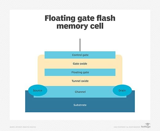
The floating gate dilemma
Flash drives have been using floating gate cells since their inception. Each cell contains one floating gate that's integrated into the cell's structure. The floating gate traps electrons when voltage is applied to the cell in a specific way and releases electrons when voltage is applied in a different way.
In a single-level cell drive, when a floating gate contains electrons, it's considered charged, or programmed, and the cell's bit value is registered as zero. Otherwise, the cell is considered uncharged, or erased, and its bit value is registered as one. The calculations are more complex for multi-level cell, triple-level cell (TLC) and quad-level cell (QLC) drives, but the fundamentals are the same.
Inside the cell, an oxide layer separates the floating gate from the silicon substrate where the voltage travels into and out of the cell. The oxide layer is thin enough for electrons to pass between the floating gate and substrate when voltage is applied. During a program -- or write -- operation, electrons move into the floating gate. During an erase operation, electrons move out of the floating gate.
Each program/erase cycle slightly damages the oxide layer, and after enough P/E cycles, the oxide layer will erode enough for electrons to start leaking out of the floating gate until it can no longer hold a charge and the cell becomes unusable.
As cell sizes shrink and more bits are packed into each cell, they become even more susceptible to damage. Technologies such as wear leveling and improvements in controller logic have helped to prolong the drive's life, but the cells will still eventually fail.
The move to 3D flash has challenged the floating gate cell more than ever. The greater the number of layers, the more difficult it becomes to manufacture and scale the chips, especially as manufacturers strive to reduce the chip's overall footprint. Some 3D SSDs now exceed 200 layers, with plans for much denser 3D flash on the horizon.
Floating gate vs. charge trap technology
Because of the limitations that come with floating gate cells, flash manufacturers such as Samsung, Micron, SK Hynix and Kioxia have turned to charge trap technologies for most of their flash storage. Charge trap cells have been around for a while, but it wasn't until 3D flash came along that vendors started looking at them seriously for enterprise-grade SSDs.
In many respects, charge trap cells work much like floating gate cells, with different voltage patterns moving electrons into and out of a trapping layer. But there's one important difference. The floating gate cell uses polycrystalline silicon to provide a conductor for trapping the electrons. The charge trap cell uses nonconductive silicon nitride to provide an insulator.
Silicon nitride is less susceptible to defects and leakage than polycrystalline silicon, and it requires lower voltage to support P/E cycles. Because of this, the charge trap cell can use a thinner oxide layer and reduce stress on the layer, which results in higher endurance rates than drives with floating gate cells. The charge trap approach also enables faster read and write operations and consumes less energy.
As floating gate cells become smaller, they also become more susceptible to disruptions, such as electrons inadvertently flowing from one floating gate to another. These disruptions can result in performance inconsistencies and lead to bad data. Because the charge trap layer is an insulator, such disruptions are less likely, which makes it possible to shrink charge trap cells smaller than floating gate cells and, as a result, produce denser drives with greater endurance.
Charge trap challenges
As promising as charge trap flash technologies sound, they do come with challenges. Electrons can become trapped, which leads to degradation. Charge trap cells can also be susceptible to data leakage, especially at higher temperatures when the electrons become more excited, although charge trap cells are still not as prone to leakage as floating gate cells.
Charge trap cells can also experience short-term data retention issues, according to Akira Goda in his article "Recent Progress on 3D NAND Flash Technologies," published in the journal Electronics. Because of the cell's design, it's possible for a trapped charge to move either laterally or vertically or to become trapped in the tunnel oxide, which can occur in a very short time.
The charge trap flash market
Despite the drawbacks that come with charge trap cells, 3D flash manufacturers are embracing the technology. They're also taking steps to address potential issues that come with charge trap cells. For example, vendors are improving their manufacturing processes, updating controller software and introducing new design features into their SSDs.
Charge trap flash has proven an effective technology for shrinking the physical size of SSDs.
Kioxia and Western Digital recently announced a 218-layer 3D flash that stores a terabyte of data using either a TLC or QLC configuration, both of which rely on charge trap cells. The complementary metal-oxide semiconductors (CMOS) use features such as wafer bonding and lateral shrinking. The flash also incorporates CMOS directly Bonded to Array (CBA) technology. With CBA, the CMOS wafer and cell array wafer are manufactured separately under optimized conditions and then bonded together, which helps to enhance bit density and deliver faster I/O speeds.
SK Hynix does something similar with its charge trap CMOS. The company recently introduced a 238-layer circuit that it calls 4D flash. The 4D in this case refers to a chip with a CMOS layer on top of a Peri Under Cell (PUC) layer, which contains the peripheral logic circuit. According to SK Hynix, the PUC technology helps to reduce the chip size and maximize production efficiency. The vendor also claims that its advanced charge trap technology improves read and write performance.
Although Micron was slower to adopt charge trap flash technology than other vendors, the company is now shipping a 232-layer NAND chip that uses it. The chip also incorporates the same type of stacked approach as the chips from Kioxia, Western Digital and SK Hynix. The array wafer is bonded to the top of the logic wafer, which Micron refers to as CMOS under array.
Samsung was one of the pioneers in 3D NAND and charge trap technologies with its line of V-NAND flash drives, which it introduced in 2013. Since then, Samsung has been a global leader in the 3D NAND industry. Samsung's current seventh-generation flash SSDs include 176 layers, but the company's eighth-generation SSDs are now in production and expected to deliver 236 layers.
The evolving world of storage
Charge trap flash has proven an effective technology for shrinking the physical size of SSDs. It's why most of today's 3D flash storage is built with charge trap cells. However, floating gate technologies have also come a long way and will likely continue to play a role in retention-sensitive uses, but their future role in 3D flash is uncertain at best.
Flash drives are denser and perform faster than ever, while their per-gigabyte price continues to drop. Most of today's flash drives are based on 3D architectures that use charge trap cells, displacing floating gate cells as the go-to technology. Because of how charge trap SSDs have proliferated, the technology is likely to be around for some time, and should continue to improve with each new generation.