Why QLC flash adoption now benefits the enterprise
While enterprises must overcome some obstacles with QLC, there is a solid case for its use. 3D NAND has played a big part in enabling QLC use within the enterprise.
Once thought to be unfit for anything but inexpensive USB flash drives, QLC flash technology has become a more viable option for enterprise SSDs.
Enterprise adoption of quad-level cell (QLC) SSDs stems from a number of factors. These include the emergence of 3D NAND, more sophisticated controllers and the fact that IT admins now have a better understanding of storage workload requirements. Together, these factors enable broader use of less staunch flash technology in cases where strength is unimportant.
3D NAND makes QLC enterprise-ready
3D NAND brought a very dramatic change to NAND flash. In the past, with planar NAND, the size of the bit cell shrank, typically by a factor of four, with every new process generation.
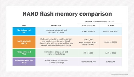
QLC flash wasn't widely available in any planar generation for a simple reason. When planar flash chips were migrated to a new process node, they were originally introduced at relaxed specifications. In the earlier generations, that would have been SLC, and at about 25nm, that became MLC. After a lot of characterization -- and once the manufacturing process had become very stable -- the industry took the next step, with the SLC chips forming the basis for MLC chips, and the chips that started out as MLC spawning TLC counterparts.
QLC flash would be a natural next step in the cost-reduction process, gaining a cost advantage of about 20% over its TLC counterparts, but this might be a couple of years after the original MLC part was introduced. By that time, the next-generation planar part would have been introduced, which would be even less costly to produce than the prior generation's QLC part. The QLC part was always just a little too late to make economic sense.
When 3D NAND was introduced, the rules changed. First, 3D NAND has a gate -- the storage element in a memory chip -- that is about 35 times as large than that of 15nm planar NAND. This enables 3D NAND to store proportionally more electrons, which makes it much easier to detect a QLC bit in 3D NAND than a TLC bit on 15nm planar NAND.
Second, most 3D NAND uses a charge trap for storage, as opposed to the floating gate used in planar NAND flash. A charge trap stores more electrons.
Finally, the gate size of 3D NAND doesn't change from one layer count to the next, so the characterization at every new process node for planar NAND is not required for 3D NAND. IT can instead focus on moving from MLC to TLC to QLC smoothly, and almost independently of layer count. This has also led suppliers to explore the possibility of penta-level cell NAND flash, with 5 bits per cell -- something that's unimaginable with planar NAND.
Treat QLC as SLC
For the reasons above, QLC flash has become a more viable, manufacturable and reasonable choice for enterprise systems. However, compared to MLC and TLC, QLC is slower, has more bit errors and offers lower endurance. That said, there are ways to overcome those obstacles.
Modern controllers use a lot of tricks to hide the fact that NAND flash has an incredibly slow write speed. One of these tricks is to tell the NAND flash chip to temporarily treat certain areas as SLC flash, enabling them to absorb data much faster than they could if they were behaving as a QLC.
The only difference between SLC, MLC, TLC and QLC bit cells is how many voltages are programmed into them -- they are all the same kind of transistor. This means IT teams can arbitrarily tell them to act as SLC, MLC, TLC or QLC, a capability that today's high-end controllers offer.
Between that and a number of older tricks, a controller can mask the differences between QLC's speed and endurance and that of SLC flash.
The industry has reached a point at which QLC flash makes sense.
The importance of controllers
The industry has reached a point at which QLC flash makes sense, thanks, in a large part, to the fact that a reasonably priced controller can manage this not-so-nice flash well enough to meet the needs of enterprise computing systems.
Moore's Law has the same effect on logic that it does on memory: prices invariably drop over time. This means that if an SSD at a certain price point includes a $1 controller, or a $10 controller, or a $100 controller, the processing power of that controller grows exponentially over time. This automatically leads to SSDs performing better some way or another. One way that they perform better is by allowing them to manage worse NAND flash than the prior generation's controllers.
Other controller advancements include the evolution of error-correction from Hamming codes to Reed-Solomon to BCH and then to low-density parity-check codes. Controllers also use improved algorithms, and even AI, to manage the SSD, and adapt and optimize operations under varying workloads.
Enterprise SSD users understand their workloads
Slow, but steady, change has occurred since SSDs first appeared in the storage marketplace.
In the early days, admins didn't really know much about their workloads and would be unpleasantly surprised when an SSD would wear out sooner than anticipated. Tools didn't exist to help admins understand what kind of traffic was being presented to the SSD. To make matters worse, application programs and even OSes weren't optimized to reduce storage to HDDs, because HDDs had no wear issues.
The early response to this was to demand SSDs with ever-increasing endurance. Some SSD makers used SLC flash for its extended life, while others doubled or even tripled the amount of flash within the drive, making only one-third of the flash visible to the system. These dramatic steps may have steeply increased SSD costs, but they provided SSDs with endurance levels as high as 25 drive writes per day (DWPD).
Over time, this trend reversed itself: admins started to understand their workloads, application programs and operating systems began to account for flash's wear, and high write load zones were set apart from those with few or no writes, enabling systems with multiple SSDs to use a mixed set of SSDs that were matched to their workload. Admins became content to save money by purchasing SSDs specified at 1 DWPD or lower.