The rise of the high-capacity vs. the high-performance SSD
Learn about the latest trends in enterprise drives, how high-performance devices figure in and the effect of advances in the underlying NAND flash technology.
Solid-state drives have mostly replaced magnetic hard disks for enterprise application workloads and are an increasingly viable option for bulk data storage. While the total number of HDDs shipped continues to outpace SDDs, the crossover in units shipped will happen in the next year or two.
SDDs offer great advantages in throughput and latency compared with HDDs. However, they haven't been able to tap the full potential of their NAND flash internals as long as they've remained compatible with HDD form factors and interfaces, notably the 2.5-inch small form factor (SFF) drive chassis and SATA I/O format. However, this situation is changing as the NVMe-based high-performance SSD, connected directly to the PCI system bus, becomes more prevalent in the enterprise.
Read on about the trends in enterprise drives, the reasons for the ascendency of NVMe devices, advances in the underlying NAND flash technology and some use cases.
SATA out, NVMe in
Statista estimates shipments of SSDs will surpass HDDs for the first time in 2021. And according to Research and Markets, the enterprise flash storage market will grow 17% annually to about $25 billion in revenue by 2024. Sales are being driven by the big-four hyperscale cloud providers -- Alibaba, AWS, Google and Microsoft -- along with co-location facilities that together are replacing many enterprise data centers.
Physics seldom gives you something for nothing, so the drawback to increasing the bit density per cell is speed and endurance.
In the past, the easiest way for flash storage to compete with hard drives in the enterprise market was to adopt existing HDD physical and interface standards. SSDs using SAS and SATA interfaces were predominant in the market until a couple of years ago. However, in late 2017, the use of NVMe high-performance SSDs exploded and surpassed the total capacity of SATA enterprise drives shipped by mid-2018.
The NVMe protocol was designed for non-volatile semiconductor memory like NAND flash and next-generation non-volatile technologies like 3D XPoint, such as Intel Optane, and resistive and magneto-resistive memories, such as those provided by Everspin and Avalanche Technology. It significantly streamlines the I/O protocol and removes other limitations of HDD protocols.
NVMe supports as many as 64K queues with as many as 64K entries versus 254 in SAS and 32 in SATA. NVMe is also optimized for multicore non-uniform memory access processors to allow multiple cores to share ownership of queues. The protocol also doesn't require I/O locking and has other features that allow performance to scale with the number of cores available in a system.
The NVMe command set is simpler and more streamlined, with less overhead than SAS or SATA, requiring half or fewer processor instructions per I/O request as HDD protocols. This efficiency translates to higher IOPS throughput and lower latency. The command set also includes advanced features such as reservations and power management that further improve system efficiency.
NVMe efficiently supports I/O virtualization technologies like single root I/O virtualization and provides extensive error reporting and management features.
According to Eric Burgener, IDC research vice president, NVMe will be the foundation for enterprise storage by 2020 and an increasing number of workloads will require NVMe for low latency, high throughput, storage density and rapid storage array rebuild times.
Denser, faster flash memory
Like dynamic RAM (DRAM), flash memory works by detecting the presence or absence of an electrical charge in a memory cell. Unlike DRAM, flash uses a storage structure that doesn't lose charge once the memory chip powers down.
Early flash designs used a floating gate of conductive polysilicon surrounded by insulating silicon dioxide to capture electrons during data writes via a process known as Fowler-Nordheim tunneling. These planar structures served the industry well for many years, but their two-dimensional structure limited the density of the memory cell array.
The solution to building higher capacity flash devices required going into the silicon substrate to etch 3D structures that could be layered to create multiple cells per pillar. These designs were combined with a change in the charge storage and insulating materials that enabled the use of a charge trap non-volatile storage mechanism.
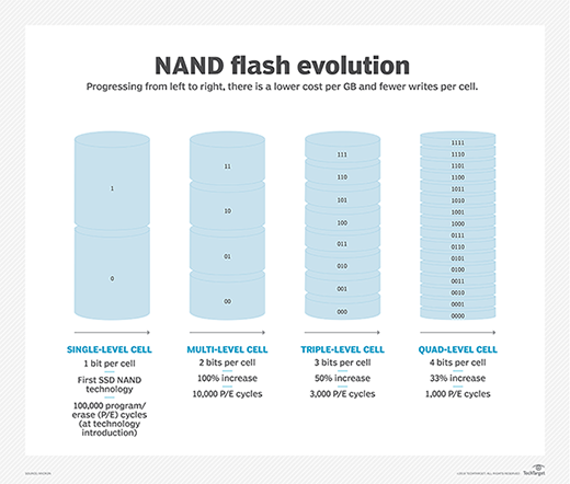
Besides layering memory cells in a 3D stack, today's devices can read multiple voltage levels per memory cell, enabling them to store more than one bit and increase capacity. In a single-level cell (SLC) NAND device, cells where the floating transistor gate is charged represents a zero and cells without a charge represent a one.
In contrast, multi-level cell (MLC) devices can apply three distinct levels of charge to the storage gate to represent four states or two bits. Over time, process tolerances and write circuitry has become accurate enough to represent seven or more states and enable triple- (TLC) and quad-level cell (QLC) devices that can store 16 voltage levels per cell.
Physics seldom gives you something for nothing, so the drawback to increasing the bit density per cell is speed and endurance. It takes progressively longer to program and read MLC, TLC and QLC devices because the programming cycle requires multiple steps. Similarly, the smaller voltage tolerances between bit states means that it takes less charge leakage before a cell is unable to distinguish between bit levels and hence is unusable. For example, most SLC devices are good for about 100,000 program/erase cycles, while a QLC device might only tolerate 100.
Usage scenarios
The trade-off between bit density and performance and endurance mean that SLC devices are preferred or outright required for write-intensive database applications, data analytics, deep learning model training or system boot drives. Conversely, TLC or QLC devices are acceptable for read-dominated applications, such as file shares and archives. SSD endurance is often specified in write-fills-per-day to indicate how many times every cell on the device can be written per day over the usable lifetime of the drive.
The ascendency of NVMe means that enterprise high-performance SSDs are now available in a variety of form factors. NVMe devices using the U.2 and U.3 standard have the same 2.5-inch SFF size as a traditional HDD but use an alternative pin-out that supports the PCIe interface. Alternatives like M.2, PCIe cards and Intel's EDSFF (aka Ruler drives) exploit the diminutive size of flash chips to provide high capacity in a compact package.
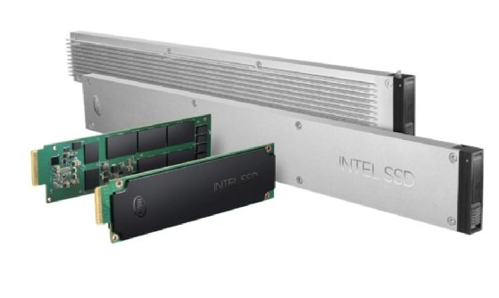
Intel's EDSFF drives
Drive capacities vary widely by cell type and form factor, but capacity-optimized QLC enterprise drives can range from 7.5 to 15.4 TB.
Next Steps
Everything you need to know about 3D NAND technology