Samsung V-NAND SSDs designed for high capacity, speed, efficiency
Samsung's V-NAND chip breaks through existing 3D NAND cell stacking limits with the industry's first 100+ layers in a move designed to enhance speed, capacity and power efficiency.
Samsung has begun mass-producing its next generation of SSDs based on V-NAND technology. The new SSDs break through current cell-stacking thresholds, offering the first drives with 3D NAND chips that exceed 100 layers of cells.
The Samsung V-NAND chips promise to deliver superior speeds and reduce power consumption, while paving the way for more layers in future-generation chips. Samsung is starting with a 250 GB SSD that targets PC OEMs, with plans to move to larger drives soon after.
How V-NAND technology works
Vertical NAND, or V-NAND, is the name that Samsung uses for its 3D NAND technology. In this architecture, the cells are stacked in multiple layers on a single NAND flash chip to increase per-chip density. Samsung's fifth-generation V-NAND chips contain from 90 to 99 layers of cells.
In a 3D NAND chip, the bit cells are stacked vertically to create a 3D structure with multiple layers. Although more layers typically mean more capacity, the number of layers is limited by the capabilities of the current technology. However, capacity can also be increased by packing more bits into each cell. In many of today's SSDs, both planar and 3D, each cell can hold three to four bits.
Prior to 3D NAND, manufacturers tried to increase per-chip densities by shrinking the cell size, making it possible to squeeze more cells into each chip. But shrinking cells can result in electrical charge leakage, leading to data corruption and diminished reliability. Layering cells is a more viable approach to greater density, while keeping the cells at a more reasonable size to prevent corruption and ensure reliability. In this way, each cell can still contain multiple bits, and each chip can contain many more cells.
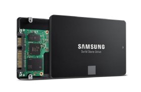
Samsung's sixth-generation V-NAND-based SSD
By building on 3D technologies, Samsung's V-NAND has been able to expand capacities without sacrificing reliability. V-NAND also improves on 3D technology in other ways. For example, it incorporates channel hole etching, an approach to layering that uses cylindrical channels to connect cells across layers by running a channel through each column of stacked cells.
V-NAND also uses charge trap flash (CTF) technology to eliminate cell-to-cell interference and electrical charge leakage, issues common to floating gate technology, the cell technology found in traditional NAND flash chips. Because CTF prevents data corruption, the drive can also use more efficient programming algorithms, which can write data as much as two times faster than NAND chips based on floating gates.
Sixth-generation Samsung V-NAND
In 2013, Samsung offered its first commercial drives that incorporated V-NAND chips. The first-generation chips started with 24 layers of CTF cells. Since then, the vendor has steadily improved V-NAND technology, with sixth-generation chips now in production. Each chip will contain more than 100 layers and provide 256 Gb of storage. Initially, Samsung will offer a 250 GB V-NAND SATA-based SSD.
Samsung plans to move into 512 Gb chips before too long and expand production of higher-speed and greater-capacity sixth-generation V-NAND drives, eventually broadening into enterprise servers.
The channel hole etching technology used in Samsung's V-NAND chip is instrumental in increasing the number of layers in the new generation of chips. When building the chips, the vendor starts with an electrically conductive mold stack for the layers and then vertically pierces them with cylindrical holes from top to bottom, resulting in uniform CTF cells across the layers.
At the same time, Samsung has reduced the number of channel holes to 670 million, compared to 930 million holes in the previous V-NAND chips, leading to a smaller chip, while improving manufacturing productivity by about 20%.
The new chips incorporate a speed-optimized circuit design to increase data transfer speeds. According to Samsung, the sixth-generation chips deliver write speeds of less than 450 microseconds and read operations of less than 45 microseconds. This new circuit design also reduces power consumption by more than 15% and minimizes the types of errors and read latencies that can occur when increasing the number of layers.
Samsung will initially target the PC OEM market with its 250 GB SATA SSD. However, the vendor has said little about when the chip might make its way into Samsung's data center SSDs.
Samsung offers four SSDs for the data center, and all of them use V-NAND chips. Two of the Samsung V-NAND drives are built for the SATA interface, and the other two use PCIe, along with the NVMe protocol, making it possible to support a wide range of workloads.
The future of V-NAND
Despite these offerings, the future of Samsung's data center SSDs remains unclear. What we do know, however, is Samsung plans to move into 512 Gb chips before too long and expand production of higher-speed and greater-capacity sixth-generation V-NAND drives, eventually broadening into enterprise servers.
Meantime, Samsung is already talking about next-generation V-NAND chips with more than 300 layers, which could involve mounting three of the current stacks. Yet, even 3D NAND technologies have their limit, and no doubt Samsung and other chip manufacturers are looking ahead to other technologies to meet the future demands of data-intensive workloads.