Choose between NAND vs. NOR flash memory
When comparing NAND flash memory to NOR, it's important to examine the structural differences to understand which type of non-volatile memory is best suited for some applications.
Whether it's a consumer shopping for a PC or an IT administrator examining SSD specifications for new servers, when most people think of flash memory, they mean NAND flash.
NAND flash has become synonymous with solid-state memory because its block addressing structure and high density make it a perfect replacement for magnetic disks. But NOR flash is another type of flash memory that has a different design topology and is better suited for some applications.
Before comparing the relative advantages and suitability of NAND vs. NOR flash for different applications, it's important to examine the structural differences.
NAND flash products -- where today's state-of-the-art, eighth-generation V-NAND memory chip boasts 1 Tb of storage capacity -- illustrate why NAND memory is the underlying component for every embedded and standalone SSD. The combination of MLC technology and 3D fabrication processes, which vertically etch NAND memory cells into a silicon substrate, has created a geometric increase in memory density and NAND chip capacity.
This article is part of
Flash memory guide to architecture, types and products
By comparison, the latest NOR flash chips can typically store up to 2 Gb, available for very fast access and high endurance that is ideal for embedded or product-centric use cases.
NAND vs. NOR circuit basics
Although NAND flash is by far the most popular of the two non-volatile memory technologies, both NAND and NOR were invented by the same Toshiba engineer in the mid-1980s. Understanding the differences and naming of the two varieties requires briefly reviewing the basics of logic gates.
NAND and NOR refer to the Boolean logic functions that are the inverse of logical AND and OR, respectively. As shown below, both NAND and NOR produce an output in response to two binary inputs.
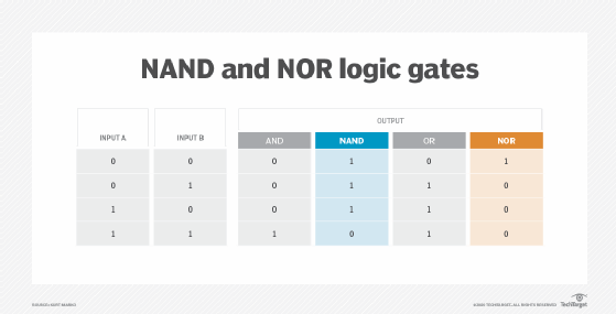
NAND and NOR logic gates simply implement the truth table above for their respective Boolean functions.
A NAND gate is conceptually implemented as an AND gate -- the output is 1 when both inputs are 1 -- followed by a NOT gate, which is a logical inversion. Likewise, a NOR gate is conceptually an OR gate -- the output is 1 when either input is 1 -- followed by the NOT gate, which is a logical inversion.
The background in Boolean logic is critical to understanding NAND and NOR flash memory because of the way flash memory cells are wired into an array of rows and columns. In NAND flash, all the cells in a group -- typically the multiple of one byte, depending on the chip's size -- share a bit line and are wired in a series with each cell connected to a separate word line. The same word line connects multiple bytes in a memory block, which is typically 4 KB to 16 KB. Thus, the bit line goes low, or zero state, only if all the word lines are high, or one state, which effectively turns the memory group into a multi-input NAND gate.
In contrast, NOR flash organizes bit lines in parallel in such a way that a memory cell only stays high, or one state, when both the bit and word lines are low, or zero state.
The series organization of NAND cells enables them to be connected by a conductive, or doped, layer on the substrate without an external contact. This significantly reduces its cross-sectional area.
The series connections of NAND flash memory cells mean they don't require the external contact -- via a metal layer -- between cells necessary for a NOR topology. Being able to connect the cells on the silicon substrate using a doping deposit means that NAND flash is often two orders of magnitude, or 100 times, denser than NOR. Also, the series connectivity of cells in a group enables them to be vertically stacked in a 3D array, with the bit line resembling a vertical pipe.
In contrast, because NOR flash cells can be addressed individually, they are faster for random-access applications. However, the dramatically lower density of NOR technology limits the sheer capacity that NOR memory devices can provide.
NOR vs. NAND product categories
These two varieties of flash memory have equally significant feature and performance differences that affect the type of applications where each is best suited. Besides capacity, NAND and NOR flash have different operating, performance and cost characteristics.
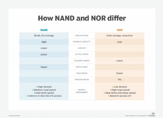
There are also several product types within each flash category, with differences in I/O interfaces, write endurance, reliability and embedded control features.
Product types within NAND flash memory
NAND flash memory stores bits per cell as SLC, meaning single-level or one bit per cell; MLC, meaning multi-level or two bits per cell; TLC, meaning triple-level or three bits per cell; quad-level, or four bits per cell; or 3D NAND, which is V-NAND where layers of cells are stacked atop one another. To determine which type of NAND is best for a workload, consider the tradeoffs between data density and reliability. For example, NAND devices with higher storage densities -- a higher number of bits per cell -- will typically exhibit lower data endurance and sturdiness.
NAND devices are just the memory chips without any of the peripheral memory controller circuitry that makes flash memory usable in an SSD, USB stick or other storage devices. In contrast, managed NAND products embed a memory controller to handle necessary functions, such as wear leveling, bad block management -- which is decommissioning nonfunctional memory blocks from use -- and data redundancy.
Product types within NOR flash memory
Serial NOR devices reduce the package pin count by only exposing a few I/O signals -- typically, one to eight. These are ideal for applications that require fast and continuous reads, such as shadow program code and granular data sets. NOR flash is commonly used in dedicated or purpose-built devices, such as thin clients, set-top boxes, printers and drive controllers.
Parallel NOR products expose multiple bytes and typically operate with memory pages rather than individual bytes. They are better suited for computer boot code and other high-capacity applications, including digital SLR cameras, memory cards and phones.
The verdict on NAND vs. NOR: Each flash type is indispensable
NAND is the workhorse of flash memory, widely used for bulk data storage in embedded systems and high-capacity storage devices such as SSDs. But NOR flash plays a critical role in storing executable boot code and for applications requiring frequent random reads of small data sets. Both types of flash memory will continue to be indispensable to the design of computer, network and storage systems.
Editor's note: This article, originally written by Kurt Marko in 2020, has been updated by TechTarget senior technology editor Stephen J. Bigelow. Kurt was a longtime TechTarget contributor who passed away in January 2022. He was an experienced IT analyst and consultant, a role in which he applied his broad and deep knowledge of enterprise IT architectures. You can explore all the articles he authored for TechTarget on his contributor page.