semiconductor fab
What is a semiconductor fab?
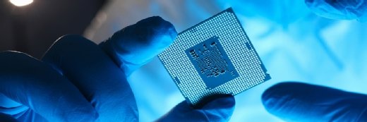
A semiconductor fab -- short for fabrication -- is a manufacturing plant in which raw silicon wafers are turned into integrated circuits (ICs). A fab lab features a clean room where ICs are etched onto wafers. The completed chips are sent to a back-end assembly and test facility before they are packaged and sold.
A semiconductor fab facility always includes a clean room -- so known because its environment is carefully controlled to eliminate dust and vibrations and to keep the temperature and humidity within a specific narrow range.
Contamination can enter the fab environment through external sources, resulting in damages to products that can affect overall yield. To minimize the losses, all potential sources of contamination are thoroughly analyzed and cleaned. For example, the tools used in the chip manufacturing process have low levels of particulates and fibers. The goal is to ensure that extraneous contamination is not introduced into the semiconductor fab to ensure the highest quality of the final products.
Various kinds of chemicals are used during the phases of the semiconductor fab process, including gases, oxidizers and acids. Some chemicals are combustible or flammable, while others are toxic, inert or pyrophoric, i.e., may ignite when exposed to air. Each chemical is properly controlled during the fab process to ensure that only desired reactions occur and to prevent them from adversely reacting during storage or disposal.
Many types of ICs are manufactured in a semiconductor fab facility, including NAND flash devices, dynamic RAM memory chips, microprocessors, graphics controllers, hard drive controllers, RAID (redundant array of independent disks) controllers and application-specific ICs. Such chips are used in a wide range of devices, such as computers, solid-state drives, hard disk drives, mobile phones, televisions and automobiles.

Photolithography in semiconductor fab labs
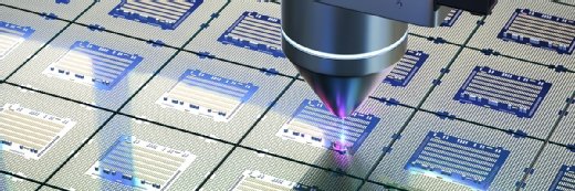
In the clean room, the ICs are etched onto wafers using photolithography. Photolithography, also known as optical lithography, is a patterning process in which parts are patterned on a thin film or a substrate, also called a wafer, which is photosensitive. A circuit pattern is photographed on this substrate, and its background is then chemically etched away.
The final output is an exposure pattern that is etched onto the material or substrate. In general, photolithography is the most common method applied to manufacture semiconductor microchips. Once the ICs are completed, they are sent for final assembly, testing, packaging and sale.
Semiconductor fabrication process
The steps in the process for semiconductor fabrication and IC manufacturing are the following.
1. Build the silicon wafer
In the first step of the fab process, the silicon wafer is built with microscopic circuit patterns etched on the chosen wafer material, such as silicon, numerous times. The wafer may have an uneven surface, which is polished using chemicals and mechanical tools. Each wafer is of uniform thickness and diameter.
2. Imprint the IC
Using photolithography, a complex pattern is transferred onto the surface of the silicon wafer. The wafer is coated with a light-sensitive substrate and then exposed to ultraviolet light through a patterned mask. The required geometric shapes are transferred to the surface of the wafer through the mask, thus creating a structure of desired shapes quickly and in a reproducible manner.
3. Etch the plasma
After the resist film is patterned by lithography, the pattern must be transferred or etched to some underlying substrate. The most common etching process used to do this is plasma etching.
In this process, a high-speed plasma substrate interacts with a gas discharge. The selected gas could be oxygen or a fluorine-bearing gas and is shot in pulses at the plasma surface. The bombardment causes the plasma surface to break down into volatile or smaller molecules, which are removed. The chemical reaction and removal of volatile molecules modify the physical properties of the plasma, making it possible to etch its parts and its entire top layer.
Apart from plasma etching, also known as dry etching, ICs can also be fabricated using wet-chemical etching. Wet-chemical etching is cheaper and easier to implement since it only uses liquid chemicals. However, this method is typically used only to etch large geometries with large diffusion rates.
4. Create the thin film
In this step, a thin film is created by densely piling up materials at atomic or molecular levels. To deposit these materials, physical vapor deposition or chemical vapor deposition methods are used. The thin film that is created consists of conducting layers made from metal materials and insulating or dielectric layers made from nonconducting materials.
5. Interconnect metals
Once the thin film is created, ions -- in the form of fine gas particles -- are deposited on it to impart the semiconductor with electric properties. Metal circuits are created to connect the film's electronic elements and enable signals to pass. The most common materials used in the metal interconnect process are aluminum and copper.
6. Conduct electrical die sorting
After the electrical circuits are drawn on the wafer and before the IC is packaged, electrical die sorting (EDS) takes place. The main goal of EDS is to improve the semiconductor's yield rate. Yield rate refers to the percentage of "good" (functional) chips relative to all the chips on a single wafer. A high yield rate is desirable because it directly affects the overall value of the chip production.
To carry out EDS, the wafer is brought into contact with a probe card that consists of numerous tiny pins. The contact between the pins and the wafer results in electrical signals going through the wafer. These signals enable defective chips to be identified. Repairable chips are marked with ink; once repairs are completed, the chips are again tested. If they fail the second test, they are discarded. EDS is important because it helps to identify defective chips, thus enabling the fab facility to save on labor, materials and time in subsequent assembly and inspection processes.
7. Package the IC
In this step, wafers are cut into individual semiconductor chips. The functional chips, which are determined after the EDS process, are placed on a lead frame. The frame ensures that electrical signals can pass between the chip and a printed circuit board to provide the electrical connections. After attaching the chips to the lead frame, they are molded by applying intense heat to a molding compound. During molding, the resin molding compound is shaped into the desired configuration of the external shell.
8. Test the IC
After packaging, the IC is tested under various temperature, humidity and voltage conditions to ensure that the chip works properly and as expected, regardless of external conditions. Testing enables the electrical and functional properties of the chip to be evaluated. It also clarifies defects that may affect product quality. Once the IC quality is confirmed, its serial number, date of manufacture and characteristics are printed on it, and the IC is sent out for sale.