NAND flash wear-out
What is NAND flash wear-out?
NAND flash wear-out is the breakdown of the oxide layer within the floating gate transistors of NAND flash memory. All of the bits in a NAND flash block must be erased before new data can be written. When the erase process is repeated enough times, it eventually breaks down the oxide layer within the floating gate transistors of the NAND flash.
Each time room must be made to write new data, a large electrical charge is used to erase the old data, eventually leading to degradation of the oxide layer in the cells.
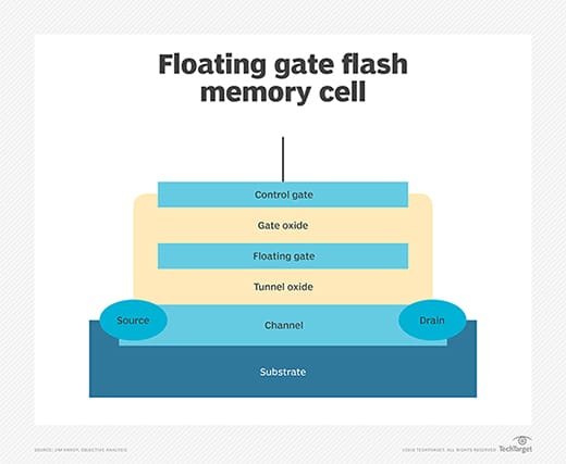
Until recently, most NAND flash storage devices relied on floating gate technology for their data cells. In this model, each data cell contains one floating gate that's integrated into the cell's structure. The floating gate plays an integral role in regulating the flow of electrons into and out of the cell's silicon substrate, a semiconductor layer that carries voltage through the cell.
An extremely thin oxide layer separates the floating gate from the silicon substrate. The electrons pass through the oxide layer as they move between the floating gate and silicon substrate. Electron movement is controlled by voltage being applied to the cell in different ways. During a programming (write) operation, electrons move into the floating gate. During an erase operation, electrons move out of the floating gate.
Each program/erase (P/E) cycle slightly damages the oxide layer. Erase operations, in particular, can be hard on NAND cells because they require a relatively large charge of electrical energy. Over time, this continuous degradation of the oxide layer can increase bit error rates. At first, these errors can be corrected with software. Eventually, however, the error correction code routines in the flash controller can't keep up with these errors, and the flash cells become unreliable.
Floating gate cells vs. charge trap cells
Because of the limitations that come with floating gates, many flash storage manufacturers have turned to other flash cell technologies, particularly charge trap flash, whose momentum has increased with the growing popularity of 3D NAND. Charge trap technology makes it possible to shrink data cells smaller than those with floating gates, resulting in greater density and endurance.
The floating gate cell and charge trap cell are structurally similar in many respects, but they differ in one important way. The floating gate is a conductor made up of polycrystalline silicon, and the charge trap is an insulator made up of silicon nitrate, which is less susceptible to defects and leakage. As a result, a charge trap cell requires less voltage and requires a thinner oxide layer. It also uses less energy, supports faster read/write operations and can deliver higher endurance.
Despite these benefits, charge trap cells come with their own challenges. For example, they might not perform as well as floating gates as the cells begin to wear. They can also be susceptible to data degradation, especially at high temperatures.
For this reason, vendors continue to look for ways to deliver flash storage that increase density, while providing the necessary endurance. Micron, for example, now offers a 176-layer NAND chip that combines charge trap technology with Micron's replacement gate architecture, which swaps out the silicon layer for highly conductive metal wordlines -- arrays of memory cells -- helping to achieve even greater density and endurance.
How long does NAND flash last?
The longevity of a NAND flash device is often discussed in terms of its endurance. Yet, the term endurance, when referring to a storage device, is defined in different ways. For example, endurance for a NAND flash drive is sometimes stated as total bytes written, or TBW, which is a product of write cycles and the logical drive capacity.
Endurance might also be expressed as the number of full drive writes per day, with one drive write being equal to the logical drive capacity. In some cases, flash endurance is defined simply as the number of P/E cycles the data cells can withstand before they can no longer store data reliably.
A number of factors contribute to a flash drive's endurance, not only the data cell technology -- i.e., floating gate vs. charge trap -- but also factors such as cell density, the physical environment and storage management techniques, such as wear leveling or overprovisioning.
Most enterprise-grade solid-state drives are designed to last between three and five years, with cell density playing a significant role in endurance rates:
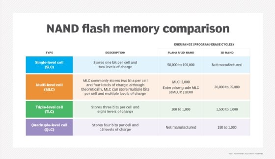
- Single-level cell (SLC): 100,000 P/E cycles
- Multi-level cell (MLC): 10,000 P/E cycles
- Enterprise MLC (eMLC): 30,000 P/E cycles
- Triple-level cell (TLC): 3,000 P/E cycles
- Quad-level cell (QLC): 1,000 P/E cycles
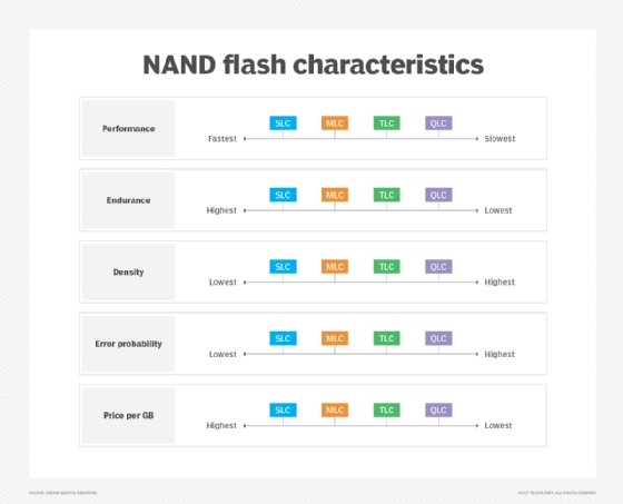
The number of P/E cycles shown here is typically cited throughout the industry as the maximum number of P/E cycles that can be expected from a drive. However, these numbers can vary substantially in practice. For example, high temperatures or inadequate wear leveling might reduce the number of P/E cycles. Regardless of the totals, however, these numbers point to an important characteristic of NAND storage: the greater the cell density, the fewer supported P/E cycles and the lower the endurance.
See also key factors that affect NAND flash memory endurance and a flash memory guide to architecture, types and products.