Toshiba, Western Digital start shift to 96-layer BiCS flash

New 96-layer 3D NAND flash memory is starting to roll out that can store more data per chip and potentially lower per-bit storage costs over 64- and 32-layer technologies.
Toshiba Memory America and Western Digital are sampling their 96-layer 3D NAND bit column stacked (BiCS) flash – formerly known as bit cost scalable – that can store four bits per cell. The capacity of a single quad-level cell (QLC) flash chip is 1.33 terabits (Tb), and a stacked 16-die package can store 2.66 terabytes (TB) of data.
Western Digital and Toshiba developed their proprietary 96-layer BiCS flash at their joint manufacturing facility in Yokkaichi, Japan. They expect to ramp up volume shipments of the 96-layer QLC 3D NAND chips later this year and eventually ship products designed for enterprise and consumer use cases requiring high-density data storage.
This week, Toshiba unveiled its first solid-state drive (SSD) based on the 96-layer, fourth-generation BiCS flash that can store three bits per cell, known as triple-level cell (TLC) flash. Toshiba’s new NVMe-based PCIe XG6 SSD primarily targets PCs, mobile computing, gaming applications and embedded systems but could also see limited use in data-center servers for boot, log and cache purposes.
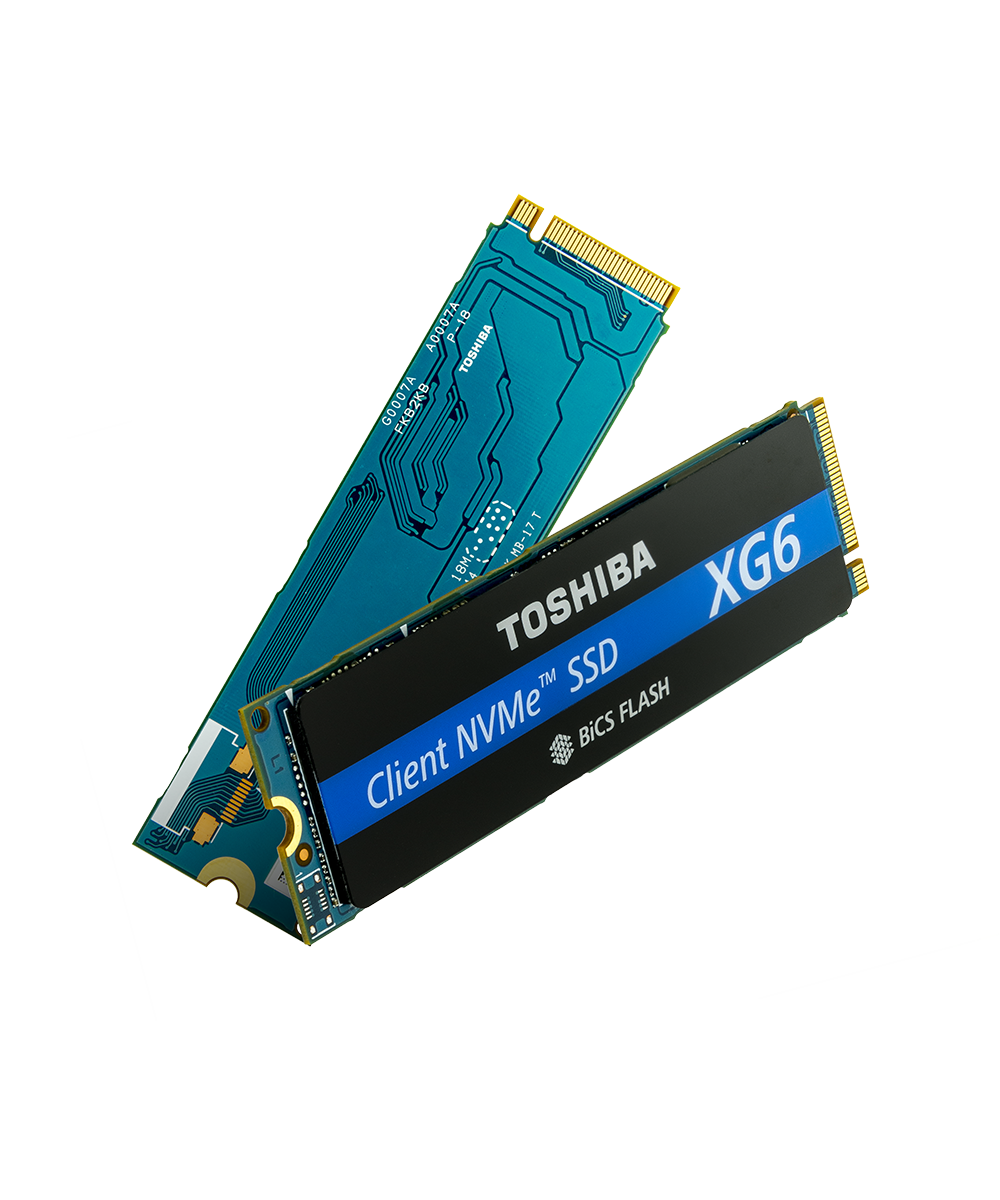
Toshiba XG5 M.2 SSD with triple-level cell (TLC) 96-layer BiCS flash
The XG6 is a single-sided 22mm-by-80 mm M.2 SSD that offers capacity options up to 1 TB and is not hot swappable. Toshiba manufactures other SSDs designed to address a broad range of enterprise and data center use cases.
The XG6 has roughly 40% higher capacity per chip unit than its predecessor XG5 model, which uses 64-layer TLC 3D NAND BiCS flash. The XG6 also improves power efficiency, at 1.2 volt I/O; offers higher interface speeds, at 667 to 800 megatransfers per second; and slightly faster read and write speeds, according to Doug Wong, a senior member of the technical staff for Toshiba Memory America.
“As die density increases over time, that will improve the likelihood that pricing will improve as well,” said Grant Van Patten, product line manager for client, OEM and data center SSDs at Toshiba. “But I think the biggest impact the 96 layer really has long term is the density. In a data center, you can have fewer racks that do just as much work. So you start to get into some of those TCO arguments.”
Toshiba is shipping initial samples of its XG6 SSD to select OEM customers and plans to showcase the new drive at next month’s Flash Memory Summit in Santa Clara, California. Toshiba also plans to show off a packaged prototype that uses the 96-layer QLC 3D NAND BiCS flash technology.
Alternative to HDDs for cold storage
Scott Nelson, senior vice president of Toshiba’s memory business unit, predicted the 96-layer QLC 3D NAND technology will have an especially significant impact in the area of cold storage, where its higher density and lower cost per GB could be a “game changer in the industry.” He said certain types of data do not require the higher performance that TLC flash can provide.
Data reads are about two to three times slower, and data writes, or programs, are about five times slower with QLC 3D NAND in comparison to TLC 3D NAND, according to Nelson.
“We’re going to see a migration from TLC to QLC. Now that’s not to say that QLC is going to replace TLC, because it will not. But there is a niche that QLC can fill,” Nelson said.
Nelson said 96-layer QLC 3D NAND could become a high-density alternative to cheaper hard disk drives (HDDs), providing faster access to cold storage.
The 96-layer QLC BiCS flash technology could account for 10% to 15% of Toshiba’s NAND chip shipments by 2019 or 2020, but 64-layer TLC 3D NAND will continue to dominate the market at that point, according to Nelson. He added that “long-tail demand” would also remain for lower density planar, or two-dimensional (2D), NAND flash. Nelson expects shipments of planar NAND based on floating gate technology to continue for the next three to five years, representing perhaps 10% of the market. Toshiba’s BiCS flash uses a charge trap memory cell.
NAND manufacturers moved from planar NAND to 3D NAND technology when they faced challenges scaling the technology. The cost of planar technology drops as the die size shrinks, and the price of 3D NAND technology falls with the addition of layers that increase the density of the chip.
Wong said the performance of TLC 3D NAND BiCS flash has been similar or better than 15-nanometer devices using planar multi-level cell (MLC), or two bits per cell, technology. He noted that Toshiba did research years ago on planar QLC NAND flash, but it didn’t make sense from a timing standpoint. He said it made more economical sense to do QLC with the BiCS flash technology because the cell size isn’t shrinking as fast and the inter-cell interference effect is lower. The 96-layer TLC and QLC 3D NAND use a similar architecture, but QLC requires stronger error correction code (ECC), Wong said.
Toshiba plans to begin shipping samples of its 96-layer QLC 3D NAND flash chips to SSD and SSD controller vendors in September. Nelson said he also expects demand from hyperscalers and tier 1 data centers that build their own SSDs.
Western Digital was unavailable for comment. The company said it is sampling the 96-layer QLC BiCS flash and expects volume shipments to start later this year, beginning with consumer products under the SanDisk brand. Western Digital eventually plans to use the QLC BiCS technology in a wide range of applications from retail to enterprise SSDs.