
Sergey Nivens - Fotolia
Key factors that affect NAND flash memory endurance
Program/erase cycles, write amplification and even garbage collection contribute to faster NAND flash wear-out. But wear leveling and bad block can help.

NAND flash memory can support only a limited number of program/erase cycles before it fails. That number, often referred to as the drive's endurance, is directly tied to the drive's expected lifespan. To maximize the lifespan, vendors employ several techniques that reduce P/E cycles and balance P/E loads, helping to prevent drives from failing prematurely.
An enterprise flash drive is typically made up of a controller, interface, dynamic RAM, multiple NAND chips and other components. The NAND flash memory stores the actual data. Each chip contains dies, each die contains planes (usually two) and each plane contains blocks. The blocks are made up of pages that include the cells where the data resides.
The cells store the data as electrons whose voltage state determines the binary values that represent the data. Most NAND flash memory uses floating gates to store the electrons, with one floating gate per cell. When a floating gate contains electrons, it is considered charged, or programmed. Otherwise, it is considered uncharged, or erased.
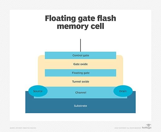
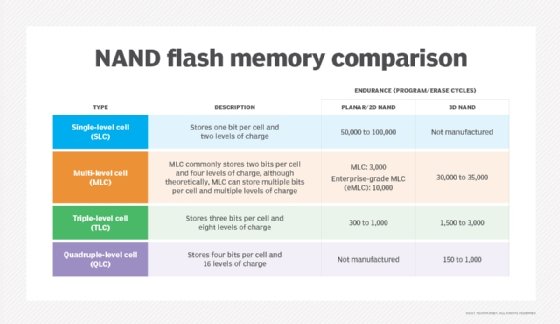
In a drive based on single-level cell technology, the drive registers the cell's bit value as zero when a floating gate is programmed and the bit value as one when the floating gate is erased. The bit values are more varied for multi-level cell (MLC) and triple-level cell (TLC) technologies, but the principle is the same.
A tunnel oxide layer separates the floating gate from the silicon substrate that carries voltage in and out of the cell. The oxide layer is thin enough for electrons to pass through when voltage is applied to the substrate. During a program (write) operation, electrons pass into the floating gate. During an erase operation, electrons move out of the floating gate.
Although this is a highly simplified explanation of what goes on in a flash cell, it points to an important concept: All program and erase operations send voltage through the substrate and cause electrons to pass through the oxide layer. Each time such an operation occurs, the oxide layer is slightly damaged. The greater the number of P/E cycles, the greater the damage to the cells.
As the oxide layer erodes, electrons are more likely to leak out of the floating gate, making it more difficult to detect the gate's actual state. Error detection and correction mechanisms can help mitigate these issues for a while, but eventually, the cell will become unreadable. These issues are further exacerbated as more bits are packed into the cells, as is the case with MLC and TLC NAND flash memory. Because of this behavior, a flash SSD can handle only a limited number of P/E cycles before the drive fails.
NAND flash memory write amplification
Because P/E cycles play such an important role in NAND flash memory longevity, the logical approach to maximizing a drive's lifespan is to minimize P/E cycles and spread the workload across all the drive's cells. But flash SSDs come with another significant challenge: write amplification.
Write amplification occurs when data modification operations result in more data being written to the flash drive than the amount being modified. Write amplification occurs in flash drives because data is read and written at the page level but can be erased only at the block level. To complicate matters, data cannot be updated directly. It must first be erased and then rewritten. The result is a lot of extra P/E cycles for each data modification operation.
For example, an update to a 10 KB text file can launch several operations. The drive must copy the block where the file's data resides to a temporary location, erase the original block of data and then write the modified data to the erased block. A simple update of a 10 KB file can easily result in 10 MB or more of data being erased and reprogrammed, eroding the tunnel oxide layer with each P/E cycle. The process becomes even more complex for larger files in which multiple blocks are involved.
Enterprise NAND flash memory must support operations such as this all day and every day, and not just for one user. What might be relatively lightweight and discrete data modifications can translate to enormous workloads that slowly deteriorate the drive's endurance.
Balancing the P/E cycles
Vendors are well-aware of how write amplification and other factors can affect NAND flash memory endurance and shorten drive lifespan. For this reason, they commonly incorporate different technologies into their drives to help minimize these issues and maximize the drive's longevity.
One of these technologies is wear leveling, a controller-based operation that distributes P/E cycles evenly across the entire disk. Wear leveling prevents individual cells from receiving an unfair share of the load, which can cause them to wear out long before the other cells and cause the drive to fail prematurely, even if most of the other cells are unused. But the wear-leveling technology is more than a simple load balancer. It is a complex algorithm that is continuously erasing and rewriting data blocks in the background, while trying to minimize excess write amplification.
Another technology that flash employs is garbage collection, a background process that moves, consolidates and erases data in order to free up blocks and improve program performance.
Unfortunately, garbage collection can also add to write amplification. Although vendors implement garbage collection in different ways, they're all trying to strike the right balance between performance and write amplification, which calls for sophisticated algorithms and careful coordination with the wear-leveling technologies.
To support operations such as wear leveling and garbage collection, NAND flash memory also includes overprovisioned space that is reserved for background processes. Wear leveling, for example, can use the free space when balancing P/E loads, and garbage collection can use the space when consolidating and moving data. Without an adequate amount of overprovisioned space, write amplification would continue to increase and performance would degrade as the drive fills with data.
NAND flash endurance
Flash drives also utilize other techniques to help extend the drive's longevity. For example, a drive might use bad block mapping to move data from a block that contains bad cells to one that contains all good cells. Some drives also incorporate data compression algorithms to help reduce the number of program operations.
SSDs are common in storage products and servers. But they can be expensive, and they do wear out. In this podcast, learn more about the technical aspects of how NAND flash storage degrades and what vendors are doing to increase SSD endurance.
Each vendor implements the drive's technologies in different ways, with the goal of minimizing P/E cycles and maximizing the drive's longevity. Vendors are also on the lookout for new ways to improve their drives, increasing performance and density, while extending the expected lifespans. The SSDs we see in a few years might have little resemblance to the flash drives of today.