cache memory

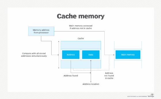
Cache memory is a chip-based computer component that makes retrieving data from the computer's memory more efficient. It acts as a temporary storage area that the computer's processor can retrieve data from easily. This temporary storage area, known as a cache, is more readily available to the processor than the computer's main memory source, typically some form of DRAM.
Cache memory is sometimes called CPU (central processing unit) memory because it is typically integrated directly into the CPU chip or placed on a separate chip that has a separate bus interconnect with the CPU. Therefore, it is more accessible to the processor, and able to increase efficiency, because it's physically close to the processor.
In order to be close to the processor, cache memory needs to be much smaller than main memory. Consequently, it has less storage space. It is also more expensive than main memory, as it is a more complex chip that yields higher performance.
What it sacrifices in size and price, it makes up for in speed. Cache memory operates between 10 to 100 times faster than RAM, requiring only a few nanoseconds to respond to a CPU request.
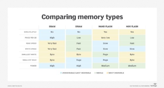
The name of the actual hardware that is used for cache memory is high-speed static random access memory (SRAM). The name of the hardware that is used in a computer's main memory is dynamic random access memory (DRAM).
Cache memory is not to be confused with the broader term cache. Caches are temporary stores of data that can exist in both hardware and software. Cache memory refers to the specific hardware component that allows computers to create caches at various levels of the network.
Types of cache memory
Cache memory is fast and expensive. Traditionally, it is categorized as "levels" that describe its closeness and accessibility to the microprocessor. There are three general cache levels:
L1 cache, or primary cache, is extremely fast but relatively small, and is usually embedded in the processor chip as CPU cache.
L2 cache, or secondary cache, is often more capacious than L1. L2 cache may be embedded on the CPU, or it can be on a separate chip or coprocessor and have a high-speed alternative system bus connecting the cache and CPU. That way it doesn't get slowed by traffic on the main system bus.
Level 3 (L3) cache is specialized memory developed to improve the performance of L1 and L2. L1 or L2 can be significantly faster than L3, though L3 is usually double the speed of DRAM. With multicore processors, each core can have dedicated L1 and L2 cache, but they can share an L3 cache. If an L3 cache references an instruction, it is usually elevated to a higher level of cache.
In the past, L1, L2 and L3 caches have been created using combined processor and motherboard components. Recently, the trend has been toward consolidating all three levels of memory caching on the CPU itself. That's why the primary means for increasing cache size has begun to shift from the acquisition of a specific motherboard with different chipsets and bus architectures to buying a CPU with the right amount of integrated L1, L2 and L3 cache.
Contrary to popular belief, implementing flash or more dynamic RAM (DRAM) on a system won't increase cache memory. This can be confusing since the terms memory caching (hard disk buffering) and cache memory are often used interchangeably. Memory caching, using DRAM or flash to buffer disk reads, is meant to improve storage I/O by caching data that is frequently referenced in a buffer ahead of slower magnetic disk or tape. Cache memory, on the other hand, provides read buffering for the CPU.
Cache memory mapping
Caching configurations continue to evolve, but cache memory traditionally works under three different configurations:
- Direct mapped cache has each block mapped to exactly one cache memory location. Conceptually, a direct mapped cache is like rows in a table with three columns: the cache block that contains the actual data fetched and stored, a tag with all or part of the address of the data that was fetched, and a flag bit that shows the presence in the row entry of a valid bit of data.
- Fully associative cache mapping is similar to direct mapping in structure but allows a memory block to be mapped to any cache location rather than to a prespecified cache memory location as is the case with direct mapping.
- Set associative cache mapping can be viewed as a compromise between direct mapping and fully associative mapping in which each block is mapped to a subset of cache locations. It is sometimes called N-way set associative mapping, which provides for a location in main memory to be cached to any of "N" locations in the L1 cache.
Data writing policies
Data can be written to memory using a variety of techniques, but the two main ones involving cache memory are:
- Write-through. Data is written to both the cache and main memory at the same time.
- Write-back. Data is only written to the cache initially. Data may then be written to main memory, but this does not need to happen and does not inhibit the interaction from taking place.
The way data is written to the cache impacts data consistency and efficiency. For example, when using write-through, more writing needs to happen, which causes latency upfront. When using write-back, operations may be more efficient, but data may not be consistent between the main and cache memories.
One way a computer determines data consistency is by examining the dirty bit in memory. The dirty bit is an extra bit included in memory blocks that indicates whether the information has been modified. If data reaches the processor's register file with an active dirty bit, it means that it is not up to date and there are more recent versions elsewhere. This scenario is more likely to happen in a write-back scenario, because the data is written to the two storage areas asynchronously.
Specialization and functionality
In addition to instruction and data caches, other caches are designed to provide specialized system functions. According to some definitions, the L3 cache's shared design makes it a specialized cache. Other definitions keep the instruction cache and the data cache separate and refer to each as a specialized cache.
Translation lookaside buffers (TLBs) are also specialized memory caches whose function is to record virtual address to physical address translations.
Still other caches are not, technically speaking, memory caches at all. Disk caches, for instance, can use DRAM or flash memory to provide data caching similar to what memory caches do with CPU instructions. If data is frequently accessed from the disk, it is cached into DRAM or flash-based silicon storage technology for faster access time and response.
Specialized caches are also available for applications such as web browsers, databases, network address binding and client-side Network File System protocol support. These types of caches might be distributed across multiple networked hosts to provide greater scalability or performance to an application that uses them.
Locality
The ability of cache memory to improve a computer's performance relies on the concept of locality of reference. Locality describes various situations that make a system more predictable. Cache memory takes advantage of these situations to create a pattern of memory access that it can rely upon.
There are several types of locality. Two key ones for cache are:
- Temporal locality. This is when the same resources are accessed repeatedly in a short amount of time.
- Spatial locality. This refers to accessing various data or resources that are near each other.
Performance
Cache memory is important because it improves the efficiency of data retrieval. It stores program instructions and data that are used repeatedly in the operation of programs or information that the CPU is likely to need next. The computer processor can access this information more quickly from the cache than from the main memory. Fast access to these instructions increases the overall speed of the program.
Aside from its main function of improving performance, cache memory is a valuable resource for evaluating a computer's overall performance. Users can do this by looking at cache's hit-to-miss ratio. Cache hits are instances in which the system successfully retrieves data from the cache. A cache miss is when the system looks for the data in the cache, can't find it, and looks somewhere else instead. In some cases, users can improve the hit-miss ratio by adjusting the cache memory block size -- the size of data units stored.
Improved performance and ability to monitor performance are not just about improving general convenience for the user. As technology advances and is increasingly relied upon in mission-critical scenarios, having speed and reliability becomes crucial. Even a few milliseconds of latency could potentially lead to enormous expenses, depending on the situation.
Cache vs. main memory
DRAM serves as a computer's main memory, performing calculations on data retrieved from storage. Both DRAM and cache memory are volatile memories that lose their contents when the power is turned off. DRAM is installed on the motherboard, and the CPU accesses it through a bus connection.
DRAM is usually about half as fast as L1, L2 or L3 cache memory, and much less expensive. It provides faster data access than flash storage, hard disk drives (HDD) and tape storage. It came into use in the last few decades to provide a place to store frequently accessed disk data to improve I/O performance.
DRAM must be refreshed every few milliseconds. Cache memory, which also is a type of random access memory, does not need to be refreshed. It is built directly into the CPU to give the processor the fastest possible access to memory locations and provides nanosecond speed access time to frequently referenced instructions and data. SRAM is faster than DRAM, but because it's a more complex chip, it's also more expensive to make.
Cache vs. virtual memory
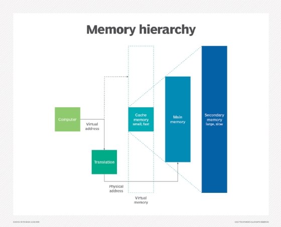
A computer has a limited amount of DRAM and even less cache memory. When a large program or multiple programs are running, it's possible for memory to be fully used. To compensate for a shortage of physical memory, the computer's operating system (OS) can create virtual memory.
To do this, the OS temporarily transfers inactive data from DRAM to disk storage. This approach increases virtual address space by using active memory in DRAM and inactive memory in HDDs to form contiguous addresses that hold both an application and its data. Virtual memory lets a computer run larger programs or multiple programs simultaneously, and each program operates as though it has unlimited memory.
In order to copy virtual memory into physical memory, the OS divides memory into page files or swap files that contain a certain number of addresses. Those pages are stored on a disk and when they're needed, the OS copies them from the disk to main memory and translates the virtual memory address into a physical one. These translations are handled by a memory management unit (MMU).
Implementation and history
Mainframes used an early version of cache memory, but the technology as it is known today began to be developed with the advent of microcomputers. With early PCs, processor performance increased much faster than memory performance, and memory became a bottleneck, slowing systems.
In the 1980s, the idea took hold that a small amount of more expensive, faster SRAM could be used to improve the performance of the less expensive, slower main memory. Initially, the memory cache was separate from the system processor and not always included in the chipset. Early PCs typically had from 16 KB to 128 KB of cache memory.
With 486 processors, Intel added 8 KB of memory to the CPU as Level 1 (L1) memory. As much as 256 KB of external Level 2 (L2) cache memory was used in these systems. Pentium processors saw the external cache memory double again to 512 KB on the high end. They also split the internal cache memory into two caches: one for instructions and the other for data.
Processors based on Intel's P6 microarchitecture, introduced in 1995, were the first to incorporate L2 cache memory into the CPU and enable all of a system's cache memory to run at the same clock speed as the processor. Prior to the P6, L2 memory external to the CPU was accessed at a much slower clock speed than the rate at which the processor ran and slowed system performance considerably.
Early memory cache controllers used a write-through cache architecture, where data written into cache was also immediately updated in RAM. This approached minimized data loss, but also slowed operations. With later 486-based PCs, the write-back cache architecture was developed, where RAM isn't updated immediately. Instead, data is stored on cache and RAM is updated only at specific intervals or under certain circumstances where data is missing or old.