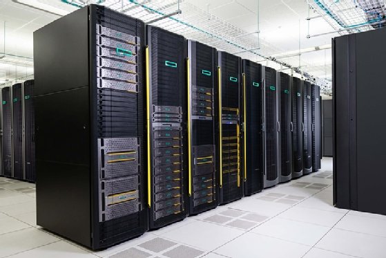
disk array
What is a disk array?
A disk array, also called a storage array, is a data storage system used for block-based storage, file-based storage or object storage. The term is used to describe dedicated storage hardware that contains spinning hard disk drives (HDDs) or solid-state drives (SSDs).
Arrays combine a series of drives into one system that can store up to petabytes of data under a central management system. Disk arrays were designed to separate storage from servers so systems could be built into large, monolithic configurations for block- or file-based storage.
How disk arrays work
A disk array enables storage capacity to scale and be managed far more efficiently than capacity from a collection of servers. Arrays have complicated redundancy features built into them, such as high-performance redundant array of independent disks (RAID) controllers, and the storage may be configured with logical unit numbers.
Disk arrays form key components of storage networks, such as storage area networks (SANs) for block storage and network-attached storage (NAS) for file storage. These networks enable storage to be managed separately from the local area network or wide area network that connects other devices inside an organization.
The disk array is the backbone of the modern business storage environment. Arrays have evolved into different designs for enterprise, midrange and small business environments and offer data protection, predictive analytics and high availability features.
They also contain controllers -- the brains of the system -- that provide a level of abstraction between the operating system (OS) and physical drives. A controller has the ability to access copies of data across physical devices and can take the form of a Peripheral Component Interconnect or PCI Express card designed to support a specific drive format, such as Serial Advanced Technology Attachment or Serial-Attached Small Computer System Interface (SCSI). Newer flash systems also support non-volatile memory express drives.
A disk array usually includes a shelf enclosure in a cabinet that holds the drives and controllers. Drives are grouped into pools, which are divided into volumes with a defined RAID level and amount of storage capacity. Applications and file systems store data in volumes. Each volume is connected to a server.
Storage arrays and flash storage
Flash or SSD storage arrays replace HDD systems inside many businesses. Flash drives offer faster performance than HDDs and often exceed the capacity that can be stored on a single spinning disk.
A flash array can read data from SSDs much faster than disk drives, and they are increasingly used to boost application performance. Storage arrays can be all-flash, all-spinning disk or hybrids combining both types of media.
But even organizations that use all-flash storage for their most important data will retain HDD systems for less performance-sensitive data, such as backups or archived data. That is because HDDs are cheaper than SSDs. Flash arrays maintain the same overall architecture as disk arrays, including connectivity to servers through switches and adapters.
An enterprise-level storage array is designed for configurations that contain hundreds of servers. It can process server compute power to handle huge amounts of data transactions per second. A midsize or low-end storage array is a stripped-down version for environments with only a few servers.
Early disk arrays required specialized components, such as field-programmable gate arrays or custom application-specific integrated circuits, to meet the performance requirements of storage networks. However, the central processing units inside most x86 servers in use today are powerful enough to handle the data protection features required in SANs without impacting performance.
SAN vs. NAS
SAN and NAS are the main types of disk arrays. SANs are designed mostly for block storage, also known as structured data inside databases. NAS systems are mainly used for file storage or unstructured data.
Besides SANs and NAS, other types of disk arrays include direct-attached storage (DAS), as well as just a bunch of disks (JBOD) and just a bunch of flash (JBOF) arrays. DAS, JBOD and JBOF arrays lack the sophisticated management of SAN and NAS arrays.
Networked storage -- SANs and NAS -- consist of storage arrays connected to application servers through fabric such as Fibre Channel (FC) or Ethernet. FC was developed specifically for SANs. Ethernet is the most common type of network connectivity and is used for NAS. SANs that don't require the performance and reliability of FC can use Ethernet through the Internet SCSI protocol.
History
The IBM 350 Disk Storage was released in 1956 as part of the IBM 305 Random Access Memory Accounting mainframe system. Other parts of the 350 system included a processing unit, printer, card punch, console and power supply.
The development of RAID techniques beginning in the 1970s and storage networking technologies helped advance the popularity of disk arrays.
RAID levels use techniques including mirroring, striping and parity to protect data stored on arrays when disks fail. OSes see RAID arrays as a single drive. RAID levels protect disk arrays in a variety of ways, balancing degrees of data protection with cost.
Networked storage began appearing in the late 1980s and advanced rapidly during the 1990s and early 2000s. In 1988, development began of the FC protocol that led to SANs. The disk SAN soon became a staple of enterprise storage. Auspex Systems brought out the first NAS systems in 1989. Network Appliance (NetApp) followed four years later and soon became the dominant NAS vendor.
While still a staple of enterprise computing, the disk array has declined in popularity a bit in recent years. Alternatives, such as flash arrays, hyper-converged infrastructure and other software-defined storage that relies on commodity servers, have become common.
Dell is the leading disk array vendor, thanks to its $60 billion-plus acquisition of EMC in 2016. Dell sells a variety of SAN and NAS disk array systems. NetApp is still among the leaders, along with Hitachi Vantara, HPE, IBM, Infinidat, Pure Storage and Qumulo.