MRAM (magnetoresistive random access memory)
What is MRAM (magnetoresistive random access memory)?
MRAM (magnetoresistive random access memory) is a method of storing data bits using magnetic states instead of the electrical charges used by devices such as dynamic random access memory (DRAM).
By combining the high speed of static random access memory (SRAM) and the high density of DRAM, MRAM promises to significantly improve electronic products by storing greater amounts of data, enabling faster data access and consuming less energy than existing electronic memory.
MRAM got its start in 1984 when Dr. Arthur Pohm and Dr. Jim Daughton were both working for Honeywell. The scientists conceived a new class of non-volatile magnetoresistance memory devices that offered random access and high density. In 1989, Daughton left Honeywell to form his own company, Nonvolatile Electronics Inc. He also entered into an agreement with Honeywell to sublicense the MRAM technology.
MRAM got a big boost in 1995 when the U.S. Defense Advanced Research Projects Agency (DARPA) provided funding to three private consortia researching the viability of making MRAM a general-purpose memory with high density, high speed and low power usage. The consortia were led by IBM, Motorola and Honeywell.
Since then, Hewlett Packard Enterprise, Matsushita, NEC, Fujitsu, Toshiba, Hitachi, Siemens and other companies have all invested in MRAM technology. Some of the most notable advancements in MRAM have come from smaller companies such as Everspin Technologies Inc. and Avalanche Technology. Everspin, for example, now has over 1,300 customers using Everspin MRAM devices in such industries as aerospace, automotive, medical devices and smart energy.
What is MRAM used for?
MRAM has been around for many years, but its adoption has been slow, in part because of manufacturing challenges, but also because the chips hold relatively little data, making them suited to only specific use cases. Even so, MRAM has been making steady inroads into a number of industries:
- Aerospace
- Defense
- Automotive
- Robotics
- Consumer electronics
- Medical devices
- Internet of things
- Edge computing
- Industrial operations and automation
- Energy management and automation
- Storage controllers and cache
- Artificial intelligence and machine learning
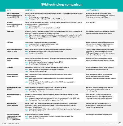
MRAM can help address the challenges of other memory technologies. It has the potential to replace both DRAM and SRAM, and it beats out NAND flash in terms of performance and durability. MRAM also consumes a relatively low-level of power, and it's resistant to radiation. As a result, MRAM could potentially benefit a number of use cases such auto powertrain systems, aircraft black boxes or medical devices such as ventilators or RFID tags.
Despite these benefits, MRAM is still an emerging technology, and it will be several years before its full potential is realized. For this reason, it's made greater gains in some industries than others, where it is still in the early development stages. But there's a good deal of interest in MRAM right now, and many companies see the technology as promising enough to warrant further research, development and investment.
How MRAM works
Unlike DRAM, which uses an electrical charge to determine if a bit is a binary 1 or 0, magnetoresistive memory uses a pair of ferromagnetic metal plates separated by a thin insulating material layer. Scientists define a metal as magnetoresistive if it shows a slight change in electrical resistance when placed in a magnetic field.
Together the two plates and insulating layer form the magnetic tunnel junction (MTJ). One plate is called the fixed layer -- or reference layer -- because it's magnetic direction never changes. The other plate is called the free layer because its magnetic direction can change when bias is applied to the MTJ. The orientation of the two magnetic fields determines whether a binary bit is a 1 or 0.
An MRAM device is made up of an array of MTJs that are connected by bit lines and word lines to form the circuitry. This is similar to how arrays of transistors in an integrated circuit make up random access memory (RAM).
The MTJ works because of a quantum phenomenon called electron tunneling. The insulating layer is only a few nanometers thick, allowing electrons to tunnel through it from one plate to the other. The degree of tunning is determined by whether the magnetic fields of each plate are oriented in parallel. When the fixed and free layers are magnetically parallel, the MTJ is in a state of low resistance. When they are not parallel, the MTJ is in a state of high resistance. Changes in the electrical resistance within the MTJ determines whether a binary bit is 1 or 0.
MRAM can perform read and write operations faster than DRAM. It also uses less power and is a non-volatile memory. For these reasons, MRAM is considered a "universal memory" that could potentially accommodate a wide range of use cases, from system computing to storage. MRAM also outshines NAND flash.
It delivers superior performance and doesn't wear out like flash. In theory, MRAM can be read from and written to until the physical material degrades.
What is STT-MRAM?
Early MRAM systems used electrical currents to induce the magnetic field in the MTJ to read or write the cell, but this approach requires more power than is ideal for modern computer systems. Today, much of the research and development effort is focused on spin transfer torque (STT) technology to read or write an MRAM cell.
Traditional MRAM devices look at the charge induced by the flow of electrons from one MTJ layer to another. In contrast, spin transfer torque MRAM (STT-MRAM) looks at the torque applied to the changeable layer by the angular momentum -- or spin -- of the electrons in the flow. Enough spin in the electron flow from one plate in the MTJ to the other can change the magnetic orientation on the second plate.
An MTJ that uses STT draws much less power than an electrically induced MTJ. In addition, STT-MRAM can be made much smaller, allowing for greater memory density in the memory devices that use it.
To perform at high speeds, however, STT-MRAM requires more power than is commercially feasible to make it a replacement for many DRAM uses. That said, STT-MRAM has begun making important inroads into DRAM territory. For example, some enterprise flash arrays now use STT-MRAM instead of DRAM as a write cache. This eliminates the need for a backup power source and power loss circuitry, which DRAM requires when used as storage cache.
What is the difference between MRAM and DRAM?
Conventional RAM computer chips such as DRAM store information as long as electricity flows through them. Once power is turned off, the information is lost unless it has been copied to a non-volatile storage. In contrast, MRAM retains data after the power supply is cut off.
Replacing DRAM with MRAM could prevent data loss and enable computers to start instantly without waiting for software to boot up.
The non-volatile nature of MRAM makes it one of its biggest selling points when compared to DRAM. However, MRAM can also deliver better read and write speeds and operate at lower voltages, and it has the potential to offer greater scalability. In addition, MRAM doesn't require periodic charge refreshes like DRAM.
Current state of MRAM
A number of commercially available MRAM products are now on the market, a trend that began in 2012 when Everspin introduced a 64 Mb STT-RAM module. (Everspin uses the acronym ST-MRAM in its product-specific marketing materials.) The Everspin module was fully compatible with the then-standard DDR3 RAM interface and packaged in a typical DDR3 form factor.
In 2013, Buffalo Americas Inc. became the first company to announce a commercial application of Everspin's ST-MRAM module, using it in a Serial Advanced Technology Attachment (SATA) III solid-state drive as cache memory.
IBM and Samsung made a joint announcement in July 2016 that they could make an MRAM device at an 11-nanometer scale. In April of that same year, Samsung announced it would have MRAM products very soon. Another important milestone came in December 2018, when Everspin shipped preproduction samples of the world's first 28 nm 1 Gb STT-MRAM chip. This was after the company had successfully commercialized its 40 nm 256 Mb STT-MRAM.
Since then, MRAM has continued on this upward trajectory. At the IEDM 2020 conference in December 2020, IBM announced the first 14 nm node STT-MRAM for addressing memory-compute bottlenecks in hybrid cloud systems. In September 2021, Avalanche Technology announced that the company would be partnering with LinearASICs on chiplets for space-grade MRAM products.